Contents
Problem
Sometimes we need highly optimized or power efficient implementation for some specific computations. However, the performance and power consumption depend on the instruction set provided by the hardware architecture. How can we find an implementation that meets the performance and power requirements?
Context
In software development, usually we rely on the general purpose processing unit for implementing the functions and the applications that we need. The implementation is achieved by composing the available instruction set following a specific order. As a result, the performance and the power are restricted by the instruction set provided by the architecture.
Although the general purpose processing unit provides high flexibility and controllability, sometimes it cannot meet the efficiency and power requirements that we expect. For example, real-time applications need to meet the real-time performance, and the mobile devices need to meet the power constraints. In such cases, we need specific instructions that are designed for high efficiency or low power. An alternative is to design a brand new hardware that meets the constraints.
The digital circuits is a hardware pattern focusing on designing hardware intellectual property (IP) or special purpose instructions for achieving the performance and power constraints that we set.
Forces
Software implementation vs. hardware implementation:
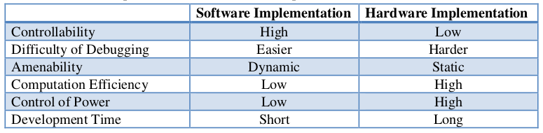
- Controllability: Software has very high controllability. It can insert/delete any operations in very short time. If the specification changes, the software implementation can be revised easily and quickly. Usually an operation in hardware is implemented by a bunch of gates. To change the control flow of hardware, we need to redesign part of the circuit, re-synthesis, re-placement, and re-route. If the specification changes after the hardware are taped-out, we might need to throw away the fabricated chips.
- Difficulty of Debugging: There are well-developed software debuggers that help software developers to find errors, while hardware developers can only rely on simulators or analyze the transition of signals to debug.
- Amenability: Recursion and dynamic memory allocation are two fundamentally powerful attributes of software that makes it more expressive than hardware. However, applications which do not call for these capabilities are amenable to hardware design. If such application demands extreme resource constraints like performance or power, then designing a dedicated piece of hardware for such application is ‘the’ most effective way to meet the design demands. A typical example of such situation is the FFT algorithm. This algorithm is the core of numerous time-critical signal processing applications and is based on data-flow model of computation requiring bounded resource only. This has resulted in hardware realization of the FFT algorithm in most of the DSP chips. Same is true for various cryptographic algorithms, eg. DES.
- Computation Efficiency: Software implementation can only use the instruction set provided by the platform for computation. It is very restricted. For hardware implementation, we are dealing with gate level components. It is possible that we can compose a sequence of computations in one clock cycle. It is also possible that we can increase the fanout of gates to increase the throughput. Therefore, hardware implementation can achieve higher performance than software implementation.
- Control of Power: It is hard for software to control the power consumption, because the software only composes the available instructions together. It can only reduce power consumption by using fewer instructions or instructions that are more power-saving. For hardware implementation, it can save power by reducing the clock frequency, turning off gates that are not running, or use gates that consume less power. Therefore, it is more flexible for hardware implementation to control power consumption.
- Development Time: The software language provides high level semantics that are easier for humans to understand. It hides most of the implementation details (like assembly codes) and provides clear and convenient interfaces for developers. As a result, software language usually can describe functionality very efficiently, which reduces the development time a lot. Moreover, the compile time of software is shorter than the synthesis, placement, and route time of hardware. The debugger of software is friendlier than hardware. These factors make the development of software easier and faster than hardware.
Solution
Hardware Implementation Specialties
Advantages of hardware implementation on parallel computations:
- Bit-level Parallelism:
Software is restricted to operate on a word size of data. In hardware, we can exploit the bit-level parallelism.
- Increase Fanout:
If there are several independent computations that take the same variable as input, we can increase the fanout of the register (assuming the variable is stored in a register) to feed in these computations concurrently. If several gates take the output of a specific gate as their input, we can also increase the fanout of the specific gate to feed the output in the other gates concurrently.
- Data Parallelism / Task Parallelism:
We can design independent hardware for independent data/tasks. Advantages of hardware implementation on serial computations:
- Alleviate Instruction Cycle Overhead:
An instruction cycle includes fetching, decoding, executing, and storing. For a computation with several operations, several instruction cycles are required. For hardware, we can read data from registers once, apply a lot of operations, and then store the results back. Therefore, only one cycle is necessary.
- Arbitrary Word Size:
The word size provided by the instruction set is fixed. For hardware implementation, we can design operations for arbitrary word size. (For example, a 128-bit adder.)
Hardware Implementation Methods
There are two ways for using hardware to implement the required functions.
1. Designing with software configurable processors (SCP)
SCP provides programmers the flexibility of redesign the instruction set they need. In some cases, the redesign of instruction set can be achieved by using annotated C/C++ code, and it is friendlier for software developers.
2. Pure hardware design
Realize the design by Application-specific integrated circuit (ASIC) or Field- programmable gate array (FPGA).
Designing with software configurable processors (SCP)
A software configurable processor [2] is a hybrid device that couples a conventional processor datapath with programmable logic to allow application programs to dynamically customize the instruction set. SCP architectures can offer significant performance gains by exploiting data parallelism, operator specialization and deep pipelining.
Here is a list of architectures that support SCP:
- 3DSP – SP5flex [3]
- Altera – NiosII [4]
- ChipWrights – CWvx Core [5]
- Context – DRL [6]
- Cradle – CT3400 [7]
- Elixent – D-Fabric [8]
- Equator – BSP-15 [9]
- Intrinsity – FastMATH [10]
- IPFlex – DAPDNA [11]
- picoChip – picoArray [12]
- QuickSilver – Adapt2400 [13]
- S6000 – Stretch [14]
- Tensilica – Xtensa LX [15]
- Triscend – Triscend A7 [16]
- Xilinx – MicroBlaze [17]
Take the Tehsilica-Xtensa architecture as an example of how SCP works [18]:
New instructions can be designed by the Tensilica Instruction Extension (TIE) language. TIE lets the designer specify the mnemonic, the encoding, and the semantics of single cycle instructions. It also lets the designer declare new processor state by using state registers. The designer can group instructions that have similar operands into classes. A class can contain one or more instructions. The behavior, or semantics, of an instruction are described using a subset of the Verilog hardware description language. Here is a simple TIE example [18]:
// define a new opcode for byteswap
opcode opcode BYTESWAP op2=4'b0000 CUST0
// declare state SWAP and ACCUM
state SWAP 1
state ACCUM 40

// map ACCUM and SWAP to user register file entries
user_register 0 ACCUM[31:0]
user_register 1 {SWAP, ACCUM[39:32]}

// define a new instruction class
iclass bs {BYTESWAP} { out arr , in ars } { in SWAP, inout ACCUM}

// semantic definition of byteswap
semantic bs {BYTESWAP} {
    wire [31:0] ars_swapped = {ars [7:0], ars[15:8],
                               ars [23:16], ars [31:24]};

    assign arr = SWAP ? ars_swapped : ars ;

    assign ACCUM = {ACCUM[39:30] + arr[31:24], ACCUM[29:20] + arr[23:16],
                    ACCUM[19:10] + arr[15:8], ACCUM[ 9: 0] + arr[7:0]};
}
The byteswap instruction conditionally reverses the byte order of the input operand and accumulates the values of the different byte lanes. The new instruction BYTESWAP can then be used in software development.
The TIE compiler automatically adds the new instructions to the RTL and the software tools. It translates the instruction semantics to the appropriate hardware description language and produces the appropriate pipeline control signals. It automatically generates the bypass control, interlock detection, and immediate generation logic required by the instructions.
The design using SCP can be summarized into 4 steps
1. Design the application in software.
2. Find the computational bottlenecks that can be sped up by hardware design.
3. Develop the special instruction set on hardware.
4. Utilize the newly designed instruction set in the original code to finalize the application.
Pure Hardware Design
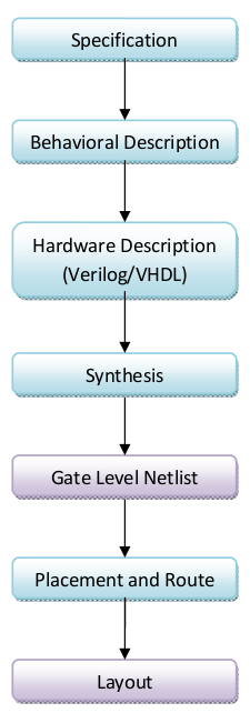
The typical design flow of the hardware can be summarized by the following graph:
- Specification
Describe the highest level of the hardware, including the functionality we want to achieve, the sketch of the overall architecture, and the interface between modules.
- Behavior Description
Describe the computation required in each module.
- Hardware Description (Verilog/VHDL)
Describe the circuits at the register transfer level. The most well known hardware languages at this level are the Verilog and VHDL.
- Synthesis
Convert the register transfer level description into gate level netlist.
- Placement and Route
Transfer the gate level netlist into physical circuits.
The synthesis and placement and route procedures are done by CAD tools and are not in the scope of this pattern. The specification and behavior description are a way too abstract that does not fit in the scope of this pattern, either. Therefore, this pattern will only introduce the hardware description languages.
The hardware description languages provide programmers to describe designs at a very abstract level. Programmers can write their RTL at an early stage. By the help of simulators, the programmers can simulate the circuit and verify the correctness of the circuit at RTL level, which is easier than debugging at gate level. The hardware design by hardware description language is analogous to software programming. A textual description with syntax, comments, and abstract semantics makes the circuit design more understandable and deliverable. Modularity also makes the code reuse for very large scale design practical. In summary, hardware description languages are now the dominant method for designing large circuits.
There are two hardware description languages that dominate the whole industry, VHDL and Verilog. Here is a brief comparison between the two languages from [1].
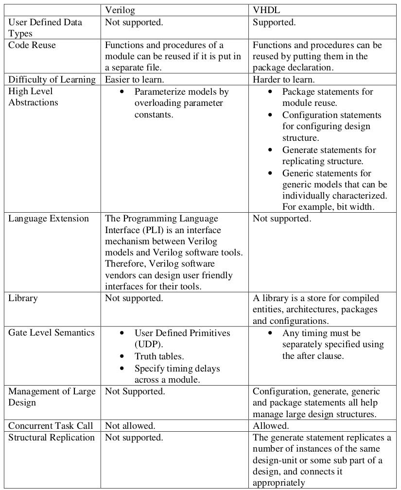
In summary, Verilog is designed for gate level design while VHDL can support higher level abstractions.
Examples
Design with SCP: Data Encryption Standard (DES) System[19]
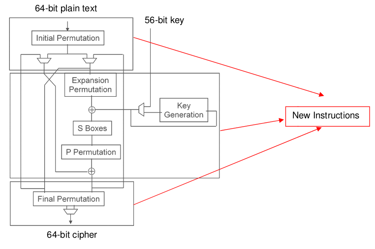
The DES system is a block cipher that was selected by NBS as an official Federal Information Processing Standard. It is used in Secure Shell (SSH) and Internet Protocol Security (IPSEC). Given a 64-bit block plain text and a 56-bit key, it will generate a 64-bit cipher using symmetric-key encryption.
The DES system can be summarized by the figure in the right [20]. IP and FP denotes the initial permutation and final permutation. The F is the Feistel function which includes four phases of encryption:
expansion, key mixing, substitution, and permutation. The ⊕ symbol
denotes the bitwise exclusive or (XOR) operation.
Now we follow the SCP 4 steps to implement the DES system [21].
1. Design the application in software.
The complete DES code is too long for an example here. We only shows the code for the permutation procedure in the Feistel function:
static unsigned permute(
    unsigned char *table,
    int n,
    unsigned int hi,
    unsigned int lo)
{
    int ib, ob; unsigned out = 0;
    for (ob = 0; ob < n; ob++) {
        ib = table[ob] - 1;
        if (ib >= 32) {
            if (hi & (1 << (ib-32))) out |= 1 << ob;
        } else {
        if (lo & (1 << ib)) out |= 1 << ob;
        }
    }
    return out;
}
2. Find the computational bottlenecks that can be sped up by hardware design.
The computational bottlenecks are the Feistel function. The C implementation requires more than a hundred of cycles to complete the computation in the Feistel function. However, all the computations can be done in one cycle using hardware implementation. The initial permutation and the final permutation can also be implemented in hardware for better performance.
3. Develop the special instruction set on hardware.
Design special instructions for the Feistel function, the initial permutation, and the final permutation.
4. Utilize the newly designed instruction set in the original code to finalize the application.
void des_encrypt(u64 *key, u64 *data){

    u64 D, K;

    K = key_permute(*key);
    D = initial_permute(*data);

    des_step(&K, &D, DES_ENCRYPT1);
    des_step(&K, &D, DES_ENCRYPT1);
    des_step(&K, &D, DES_ENCRYPT2);
    des_step(&K, &D, DES_ENCRYPT2);
    des_step(&K, &D, DES_ENCRYPT2);
    des_step(&K, &D, DES_ENCRYPT2);
    des_step(&K, &D, DES_ENCRYPT2);
    des_step(&K, &D, DES_ENCRYPT2);
    des_step(&K, &D, DES_ENCRYPT1);
    des_step(&K, &D, DES_ENCRYPT2);
    des_step(&K, &D, DES_ENCRYPT2);
    des_step(&K, &D, DES_ENCRYPT2);
    des_step(&K, &D, DES_ENCRYPT2);
    des_step(&K, &D, DES_ENCRYPT2);
    des_step(&K, &D, DES_ENCRYPT2);
    des_step(&K, &D, DES_ENCRYPT1);
    *data = final_permute(D);
}
The overall structure of the design can be summarized as:
Pure Hardware Design: Greatest Common Divisor (GCD) [1]
The algorithm used to solve the GCD problem is summarized in the following diagram:
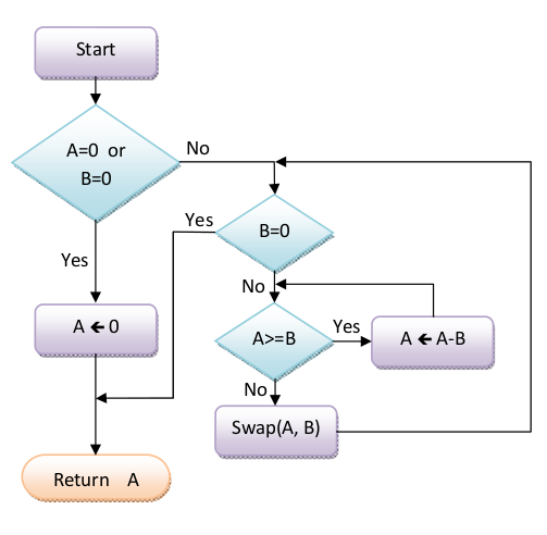
The algorithm is based on the equation GCD(A, B) = GCD(B, A mod B). The remainder calculation A mod B is achieved by subtracting B from A until A is less than B.
Here we present the implementation of the GCD problem on C, VHDL, and Verilog languages [1].
C implementation:
    #include <stdio.h> main ()
    {
        int A_in, B_in, A, B, Swap, Y, Y_Ref, Passed;
        FILE *file_pointer;
        file_pointer = fopen("gcd_test_data.txt", "r");
        Passed = 1;
        while (!feof(file_pointer))
        {
            /*------------------------------------*/
            /* Read test data from file */
            /*------------------------------------*/
            fscanf (file_pointer, "%d %d %d\n", &A_in, &B_in, &Y_Ref);
            /*----------------------------------*/
            /* Model GCD algorithm */
            /*----------------------------------*/
            A = A_in;
            B = B_in;
            if (A != 0 && B != 0)
            {
                while (B != 0)
                {
                    while (A >= B)
                    {
                        A = A - B;
                    }
                    Swap = A;
                    A = B;
                    B = Swap;
                }
            }
            else
            {
                A = 0;
            }
            Y = A;
            /*------------------------------*/
            /* Test GCD algorithm */
            /*------------------------------*/
            if (Y != Y_Ref)
            {
                printf ("Error. A=%d B=%d Y=%d Y_Ref= %d\n", A_in, B_in, Y, Y_Ref);
                Passed = 0;
            }
        }

        if (Passed = 1) printf ("GCD algorithm test passed ok\n");
    }
VHDL algorithmic level implementation:
library STD;
    use STD.TEXTIO.all;
    entity GCD_ALG is
    end entity GCD_ALG;
    architecture ALGORITHM of GCD_ALG is
    --------------------------------------------
    -- Declare test data file and results file
    --------------------------------------------
    file TestDataFile: text open
        read_mode is "gcd_ test_data.txt";
    file ResultsFile: text open write_mode is
        "gcd_alg _test_results.txt";
    begin
        GCD: process
            variable A_in, B_in, A, B, Swap, Y, Y_Ref: integer range 0 to 65535;
            variable TestData: line;
            variable BufLine: line;
            variable Passed: bit := '1';
    begin
        while not endfile(TestDataFile) loop
        -------------------------------------
        -- Read test data from file
        -------------------------------------
        readline(TestDataFile, TestData);
        read(TestData, A_in);
        read(TestData, B_in);
        read(TestData, Y_Ref);
        ------------------------------------
        -- Model GCD algorithm
        ------------------------------------
        A := A_in; B := B_in;
        if (A /= 0 and B /= 0) then
            while (B /= 0) loop
                while (A >= B) loop
                    A := A - B;
                end loop;
                Swap:= A;
                A := B;
                B := Swap;
            end loop;
        else
            A := 0;
        end if;
        Y := A;
        ---------------------------------
        -- Test GCD algorithm
        ---------------------------------
        if (Y /= Y_Ref) then -- has failed
            Passed := '0';
            write(Bufline, st ring'("GCD Error: A=")); write(Bufline, A_in);
            write(Bufline, string'(" B="));
            write(Bufline, B_in);
            write(Bufline, string'(" Y="));
            write(Bufline, Y);
            write(Bufline, string'(" Y_Ref="));
            write(Bufline, Y_Ref);
            writeline(ResultsFile, Bufline);
        end if;
      end loop;
    if (Passed = '1') then -- has passed
        write(Bufline, string' ("GCD algorithm test has passed"));
        writeline(ResultsFile, Bufline);
    end if;
   end process;
  end architecture ALGORITHM
Verilog algorithmic level implementation:
module GCD_ALG;
parameter Width = 8;
reg [Width-1:0] A_in, B_in, A, B, Y, Y_Ref;
reg [Width-1:0] A_reg,B_reg,Swap;
parameter GCD_tests = 6;
integer N, M;
reg Passed, FailTime;
integer SimResults;
// Declare memory array for test data
// ----------------------------------
reg [Width-1:1] AB_Y_Ref_Arr[1:GCD_tests*3];
//----------------------------------
// Model GCD algorithm
//----------------------------------
always @(A or B)
    begin: GCD
        A = A_in;
        B = B_in;
        if (A != 0 && B != 0)
            while (B != 0)
                while (A >= B) begin
                    A = A - B;
                    Swap = A;
                    A = B;
                    B = Swap;
                end
        else
            A = 0;
            Y = A;
    end
//------------------------------
// Test GCD algorithm
//-----------------------------
initial begin
// Load contents of
// "gcd_test_data.txt" into array.
$readmemh("gcd_test_data_hex.txt", AB_Y_Ref_Arr);
// Open simulation results file SimResults = $fopen("gcd.simres");
Passed = 1;
// Set to 0 if fails
for (N=1; N<=GCD_tests; N=N+1) begin
    A_in = AB_Y_Ref_Arr[(N*3)+1];
    B_in = AB_Y_Ref_Arr[(N*3)+2];
    Y_Ref=AB_Y_Ref_Arr[(N*3)+3];
    #TestPeriod
    if (Y != Y_Ref) begin // has failed
        Passed = 0;
        $fdisplay (SimResults, " GCD Error:
            A=%d B=%d Y=%d. Y should be %d", A_in, B_in, Y, Y_Ref);
    end
end
if (Passed == 1) // has passed
    $fdisplay (SimResults, "GCD algorithm test ha s passed");
    $fclose (SimResults);
    $finish;
end
endmodule
VHDL RTL implementation:
    library IEEE;
    use IEEE.STD_Logic_1164.all, IEEE.Numeric_STD.all; entity GCD is
    generic (Width: natural);
    port (Clock,Reset,Load: in std_logic;
        A,B: in unsigned(Width-1 downto 0);
        Done: out std_logic;
        Y: out unsigned(Width-1 downto 0));
    end entity GCD;
    architecture RTL of GCD is
        signal A_New,A_Hold,B_Hold: unsigned(Width-1 downto 0);
        signal A_lessthan_B: std_logic;
    begin
    ----------------------------------------------------
    -- Load 2 input registers and ensure B_Hold < A_Hold
    ---------------------------------------------------
    LOAD_SWAP: process (Clock)
    begin
        if rising_edge(Clock) then if (Reset = '0') then
            A_Hold <= (others => '0');
            B_Hold <= (others => '0');
        elsif (Load = '1') then
            A_Hold <= A;
            B_Hold <= B;
        else if (A_lessthan_B = '1') then
            A_Hold <= B_Hold;
            B_Hold <= A_New;
        else A_Hold <= A _New;
        end if;
    end if;
    end process LOAD_SWAP;
    SUBTRACT_TEST: process (A_Hold, B_Hold)
    begin
        -------------------------------------------------------
        -- Subtract B_Hold from A_Hold if A_Hold >= B_Hold
        ------------------------------------------------------
        if (A_Hold >= B_Hold) then
            A_lessthan_B <= '0';
            A_New <= A_Hold - B_Hold;
        else
            A_lessthan_B <= '1';
            A_New <= A_Hold;
        end if;
        -------------------------------------------------
        -- Greatest common divisor found if B_Hold = 0
        -------------------------------------------------
        if (B_Hold = (others => '0')) then
            Done <= '1';
            Y <= A_Hold;
        else
            Done <= '0';
            Y <= (others => '0');
        end if;
    end process SUBTRACT_TEST;
    end architecture RTL;
Verilog RTL implementation:
module GCD (Clock, Reset, Load, A, B, Done, Y);
parameter Width = 8;
input Clock, Reset, Load;
input [Width-1:0] A, B;
output Done;
output [Width-1:0] Y;
reg A_lessthan_B, Done;
reg [Width-1:0] A_New, A_Hold, B_Hold, Y;
//-----------------------------------------------------
// Load 2 input registers and ensure B_Hold < A_Hold
//-----------------------------------------------------
always @(posedge Clock) begin: LOAD_SWAP
    if (Reset) begin
        A_Hold = 0;
        B_Hold = 0;
    end
    else if (Load) begin
        A_Hold = A;
        B_Hold = B;
    end
    else if (A_lessthan_B) begin
        A_Hold = B_Hold;
        B_Hold = A_New;
    end
    else
        A_Hold = A_New;
    end
always @(A_Hold or B_Hold)
    begin: SUBTRACT_TEST
        //--------------------------------------------------
        // Subtract B_Hold from A_Hold if A_Hold >= B_Hold
        //--------------------------------------------------
        if (A_Hold >= B_Hold) begin
            A_lessthan_ B = 0;
            A_New = A_Hold - B_Hold;
        end
        else begin
            A_lessthan_B = 1;
            A_New = A_Hold;
        end
        //----------------------------------------------
        // Greatest common divisor found if B_Hold = 0
        //----------------------------------------------
        if (B_Hold == 0) begin
            Done = 1;
            Y = A_Hold;
        end
        else begin
            Done = 0;
            Y = 0;
        end
    end
    endmodule
Known Uses
- The digital circuits pattern is widely used in all hardware design, including ASIC and FPGA.
- The SCP based approach is used in embedded system, such as data encryption and decryption, video encoding and decoding, and computer network protocols.
Related Patterns
- Circuits: If a problem can be described as a circuit in natural, it can be implemented by hardware.
- Spectral Methods: FFT can be implemented by hardware.
- Task Parallelism: Heterogeneous system is an example of task parallelism on hardware.
- Data Parallelism: SIMD is a specific instruction set provided by hardware.
References
[1] Smith, D. J. 1996. VHDL & Verilog compared & contrasted—plus modeled example written in VHDL, Verilog and C. In Proceedings of the 33rd Annual Conference on Design Automation.
[2] Arnold, J. M. 2006. Software Configurable Processors. In Proceedings of the IEEE 17th international Conference on Application-Specific Systems, Architectures and Processors. [3] http://www.3dsp.com/pdf/3dsp_sp5flex.pdf
[4] http://www.altera.com/literature/hb/nios2/n2cpu_nii51002.pdf
[5] http://www.chipwrights.com/tech/bg.html
[6] http://www.contextdrl.com/technologies.html
[7] http://www.cradle.com/ftp/pub/marcom/ct3400_DataSheet.pdf
[8] http://www.elixent.com/products/technologies.htm
[9] http://equator.com/productsservices/pdf/BSP-15.pdf
[10] http://www.intrinsity.com/technology/docs/public/FastMATH_Data_Sheet.pdf
[11] http://www.ipflex.com/en/E1-products/dd2Arch.html
[12] http://www.commsdesign.com/story/OEG20021202S0059
[13] http://www.qstech.com/pdfs/Adapt2400_Whitepaper_0404.pdf
[14] http://www.stretchinc.com/_files/s6ArchitectureOverview.pdf
[15] http://tensilica.com/xtensa_LX_final.pdf
[16] http://www.easic.com/news_events/DesignCon.2002.PBDPanel.gmartin.pdf
[17] http://www.xilinx.com/ipcenter/processor_central/microblaze/architecture.htm
[18] Gonzalez, R.E., Xtensa: a configurable and extensible processor, Micro, IEEE , vol.20, no.2, pp.60-70, Mar/Apr 2000
[19] National Bureau of Standards, Data Encryption Standard, FIPS-Pub.46. National Bureau of Standards, U.S. Department of Commerce, Washington D.C., January 1977.
[20] http://en.wikipedia.org/wiki/Data_Encryption_Standard
[21] http://bwrc.eecs.berkeley.edu/Classes/CS252/Notes/xtensa_022400.pdf
Author
Author: Bor-Yiing Su
Shepherd: Sayak Ray